Board design
KiCad sources, schematics, PCB versions and fabrication outputs
Board design
The board has been designed with KiCad. Both KiCad 7.x and 8.x have been used during the development.
The KiCad sources live in this repository under mds-hardware/, split into two projects:
mds-hardware/network_player/— the main boardmds-hardware/dac/— the audio DAC daughter board
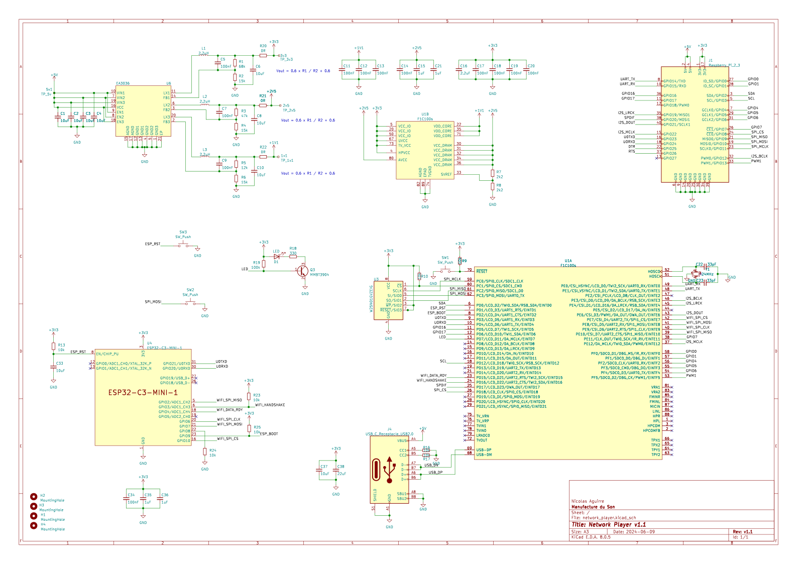
Schematics
A rendered SVG of the schematics is included for quick reference:
Versions
| Version | Date | Status | Schematic | PCB | Gerbers |
|---|---|---|---|---|---|
| v1 | 2024-01-15 | Sent to JLCPCB, had routing issues | ZIP | ||
| v1.1 | 2024-06-02 | Sent to JLCPCB, fixes routing issues of v1 | ZIP | ||
| v2 | 2024-10-17 | Full redesign on Allwinner T113-s3, never produced | ZIP |
Latest produced version: v1.1
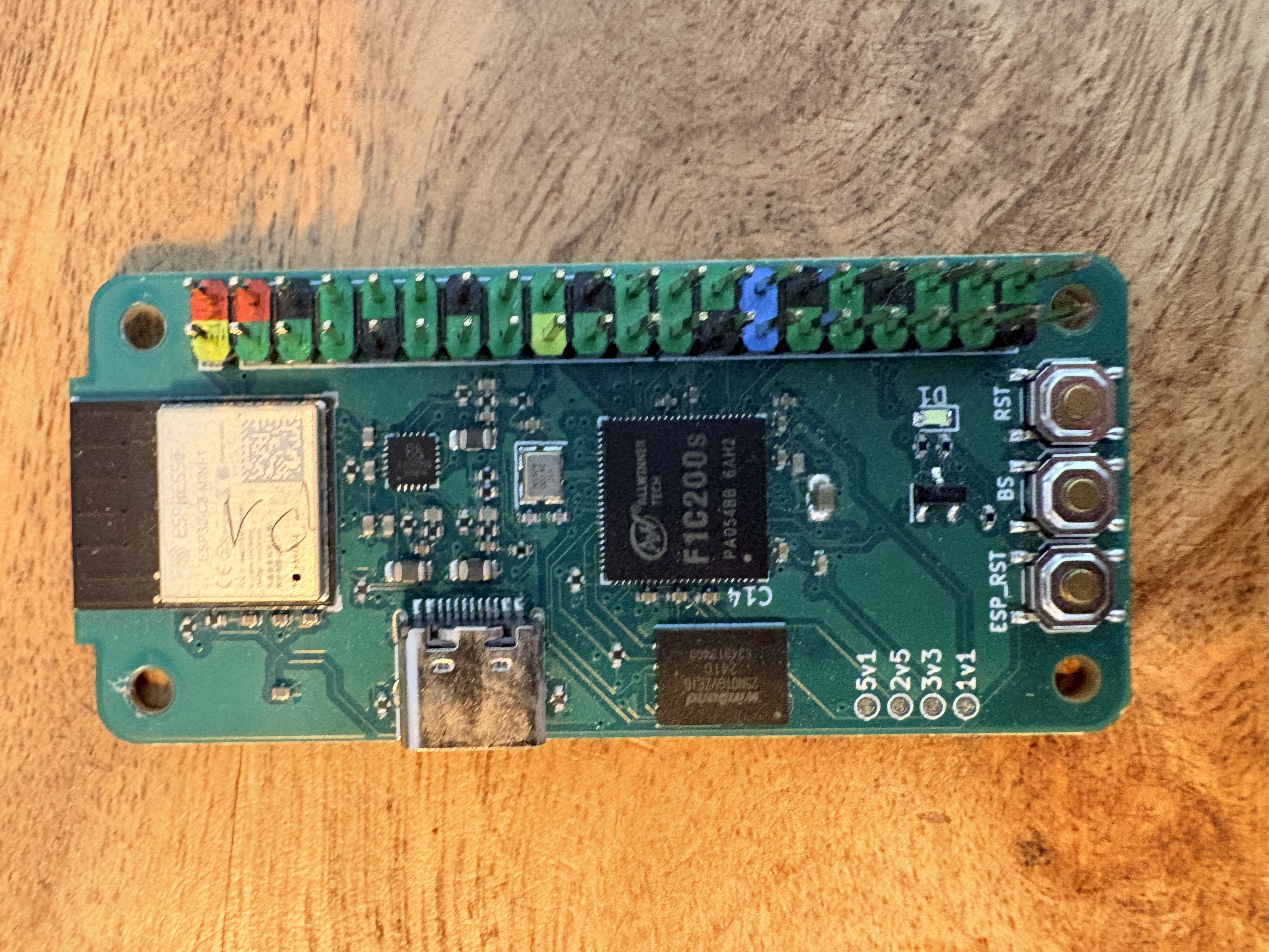
v1.1 is the version that was actually fabricated and assembled by JLCPCB. Compared to v1, it brings the following changes:
- Removed the discrete transistors used for ESP32 boot/reset, driven directly from F1C200s GPIOs instead
- EA3036 enable pin tied to 3.3 V
- Added a RST button that pulls the MISO line to ground to disable booting from flash
- ESP32 moved to SPI1; SPI0 is now shared between the NAND flash and the RPi connector
Assembled boards
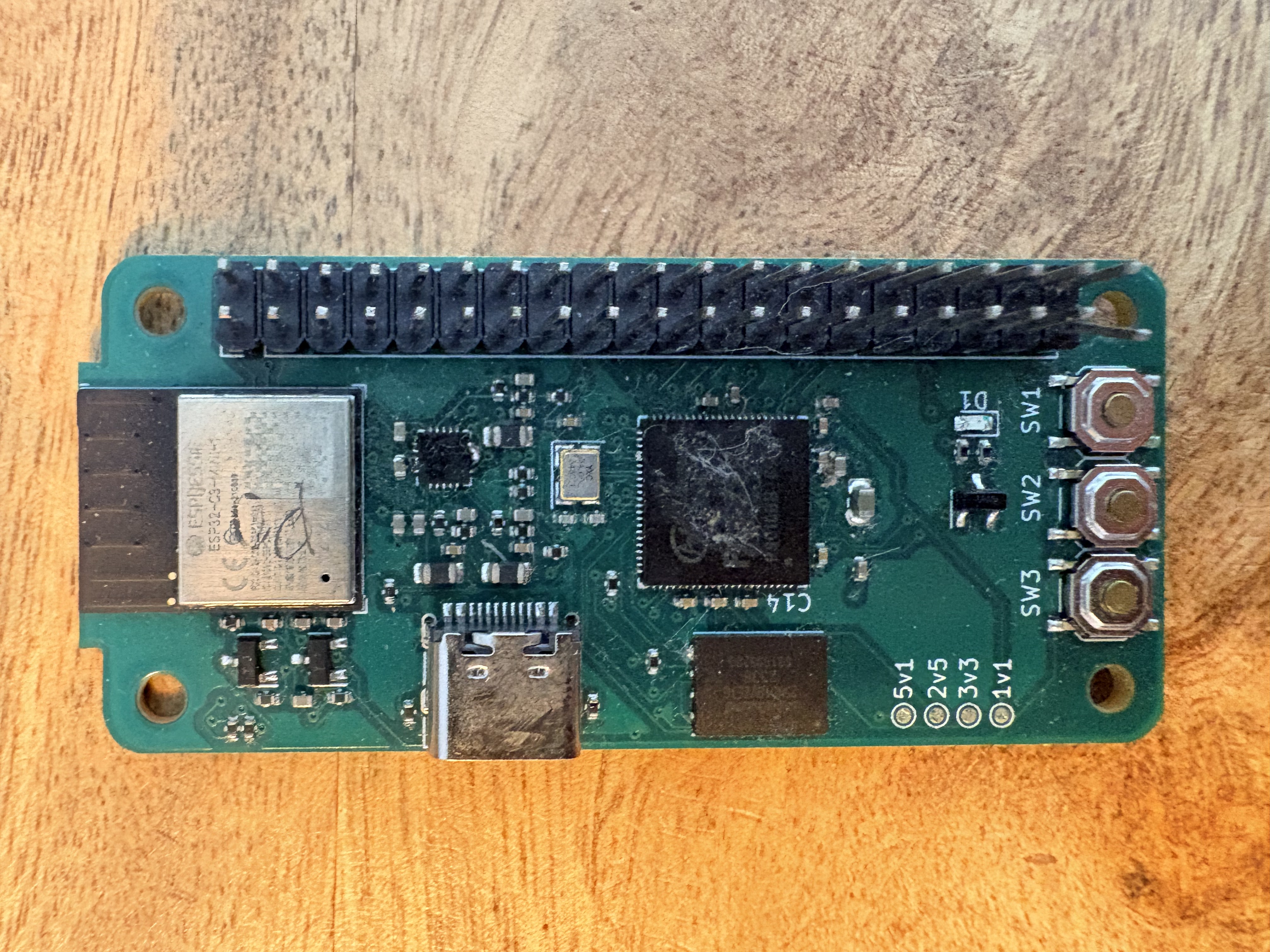
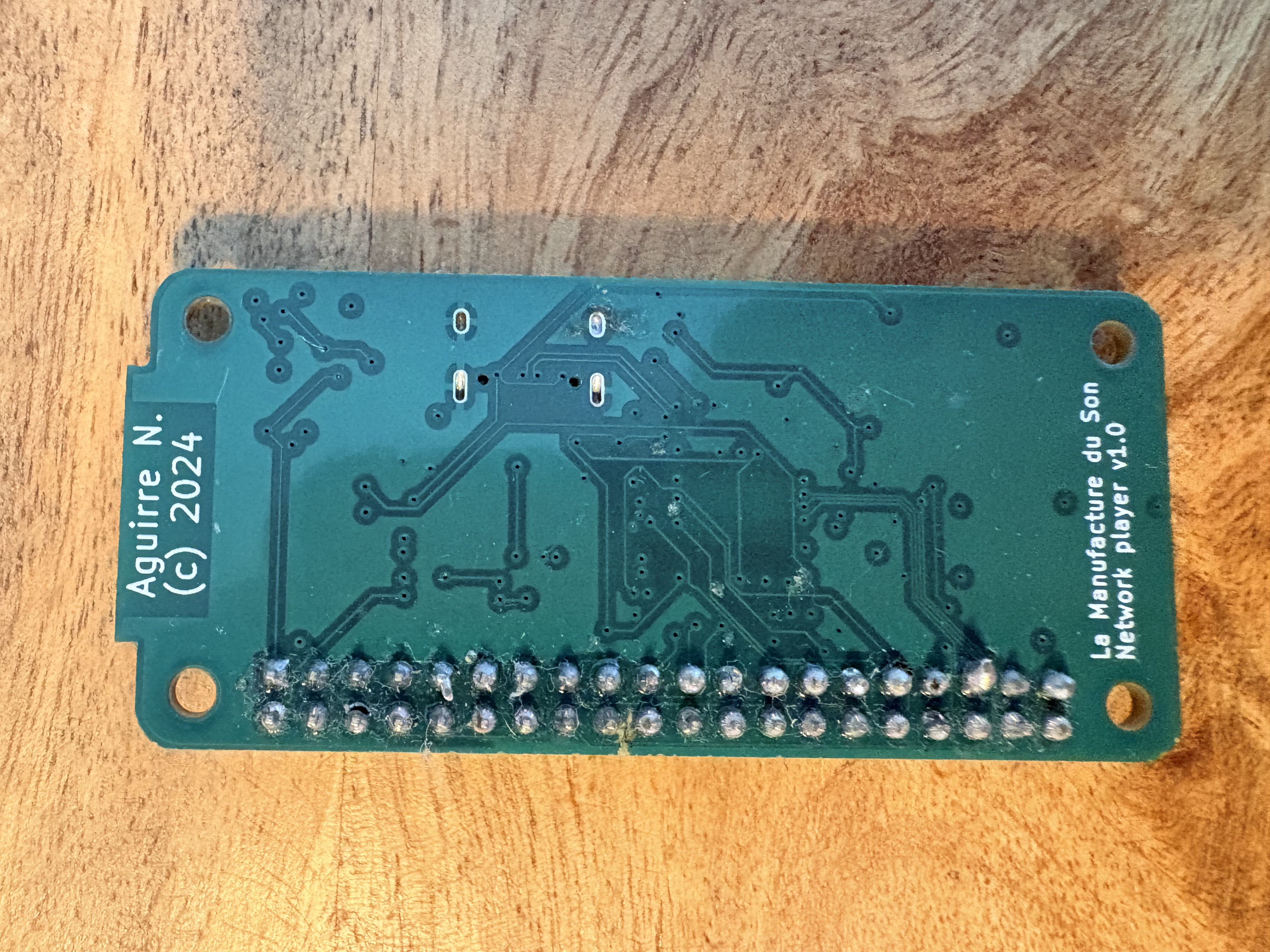
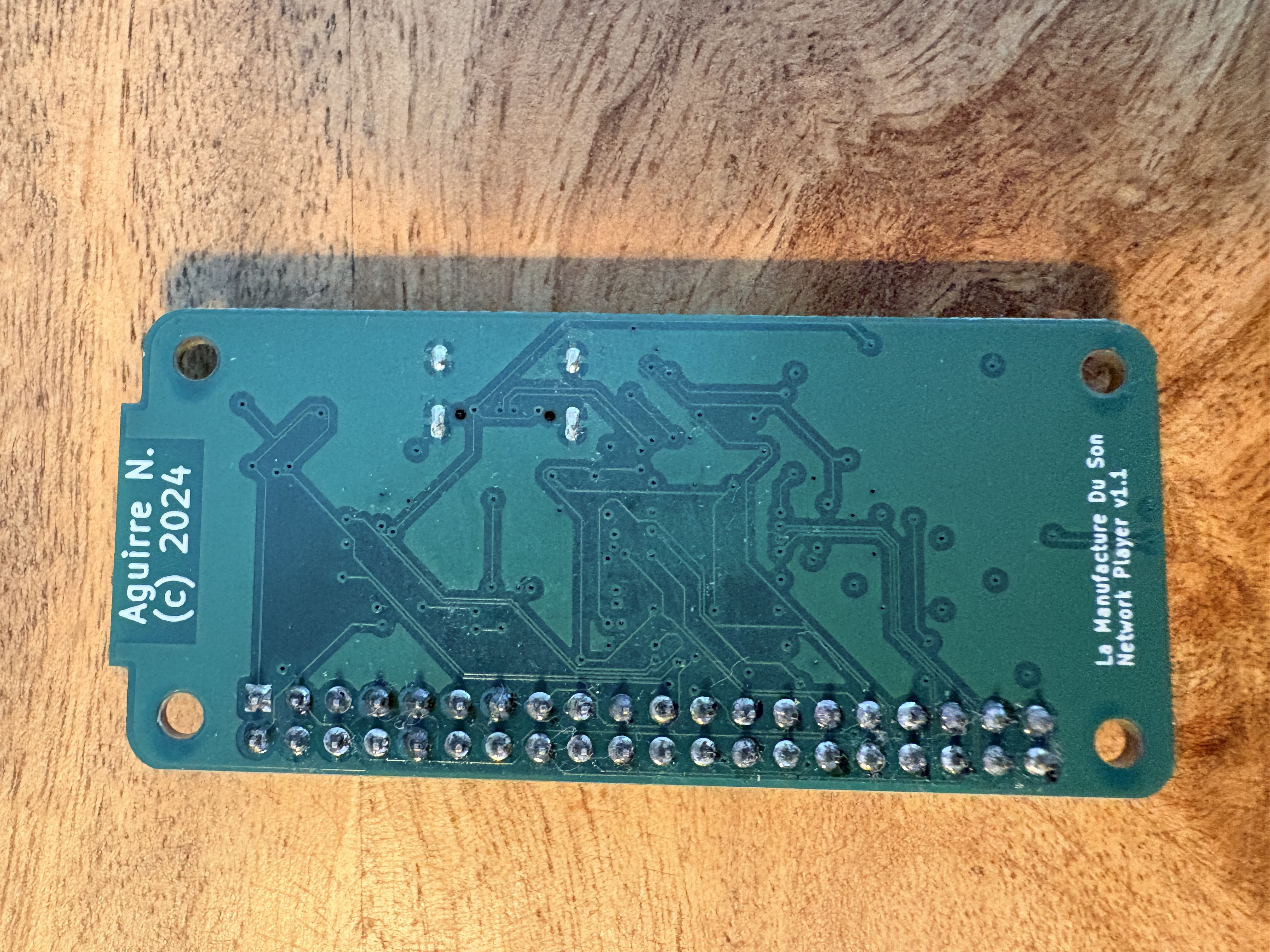
The v1.1 board as assembled by JLCPCB:
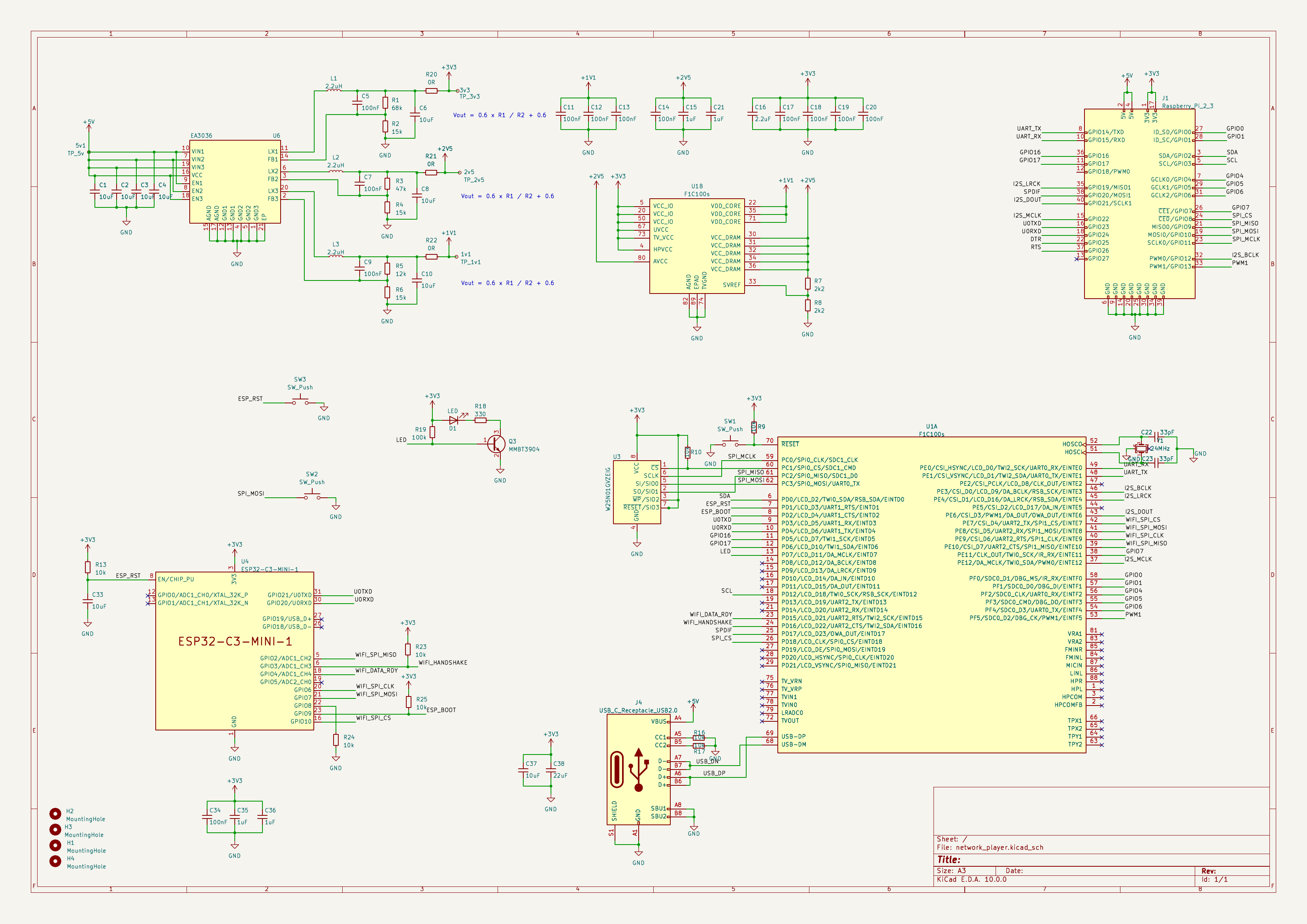
For reference, the earlier v1 board: